What’s in the blog:
Introduction:
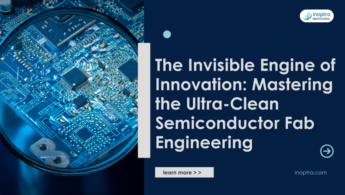
In the race to power the next generation of technology—from AI to electric vehicles—the spotlight is on transistor counts. But behind every microscopic breakthrough lies a macro-scale engineering marvel: the semiconductor fabrication plant, or “fab.” Here, the battle for purity is relentless, and the ultra-clean environment is the unsung hero that makes it all possible. This is where engineering excellence meets atomic-level precision.

1. The Non-Negotiable Standard of Purity
Semiconductor manufacturing operates on a scale where a single particle, smaller than a virus, can spell disaster for a chip worth thousands of dollars. Fab cleanrooms are maintained to ISO Class 1-5 standards, meaning they are hundreds to thousands of times cleaner than a hospital operating room. In this world, air, temperature, and vibration are not just environmental factors; they are critical process parameters. The integrity of this controlled environment is not an accessory to production—it is the very foundation.

2. The Core Engineering Hurdles in a Modern Fab
Maintaining this pristine state presents a unique set of challenges that blend facility management with process engineering:
- Infrastructure and Legacy Systems:Many existing fabs are built on aging systems that are less energy-efficient and struggle to meet the stringent demands of next-gen nodes. Retrofitting for higher performance without disrupting production is a massive undertaking.
- Scalability and Agility:The rapid pace of technological change demands cleanrooms that can adapt. Traditional builds have long lead times and rigid structures, clashing with the need for scalable, flexible manufacturing capacity.
- The Human Factor:Even with advanced automation, skilled engineers and technicians are essential. Their training and strict adherence to protocols are the first line of defence against “environmental drift” and contamination.
- The Sustainability Imperative:Ultra-clean environments are incredibly energy-intensive. Balancing the uncompromising need for cleanliness with the growing mandate for energy efficiency and reduced carbon footprint is a key strategic challenge.
3. Engineering a Resilient Future: Best Practices
Overcoming these hurdles requires a forward-thinking approach grounded in robust engineering principles:
- Embrace Modular and Flexible Design:Modular cleanroom components allow for faster expansion, reconfiguration, and upgrades, enabling fabs to scale and adapt to new processes with minimal downtime.
- Automate to Eliminate Contamination:Automated Material Handling Systems (AMHS) and robotics minimize human interaction with wafers, directly reducing the largest source of particulate contamination.
- Implement Smart, Real-Time Monitoring:Move from reactive to proactive control with advanced sensors and data analytics. Real-time monitoring of particles, temperature, and humidity allows for immediate correction before a parameter drifts out of spec.
- Foster Cross-Functional Collaboration:Siloed teams are a liability. A seamless integration between process, facility, and equipment engineers ensures that the cleanroom is designed and managed as a holistic, high-performance system.

4. The Strategic Advantage in a Growing Global Market
As semiconductor manufacturing expands globally into new regions, the ability to establish and maintain high-yield, ultra-clean environments becomes a powerful competitive differentiator. The engineering decisions made today—in design, technology, and process—will directly define a fab’s operational efficiency, uptime, and profitability for years to come.
Engineering Purity for Performance and Profitability
In semiconductor manufacturing, ultra-clean environments aren’t optional—they’re the backbone of yield, reliability, and competitive advantage. Every particle eliminated, every vibration controlled, and every airflow optimized translates directly into higher throughput and lower scrap rates. The fabs that win tomorrow will be those that integrate precision engineering, modular scalability, and intelligent automation today.
InOpTra delivers exactly that.
- Modular Cleanroom Solutions for rapid deployment and future-proof scalability
- Advanced Contamination Control Systems powered by real-time monitoring and predictive analytics
- Energy-Efficient Infrastructure that meets sustainability mandates without compromising ISO Class 1–5 standards
Whether you’re building a greenfield fab or upgrading legacy systems, InOpTra helps you design and implement environments that maximize uptime, minimize risk, and accelerate time-to-market. With deep expertise and proven execution, we don’t just build cleanrooms—we engineer strategic assets that drive profitability.
Ready to transform your fab into a high-performance, ultra-clean powerhouse?
Partner with InOpTra to turn engineering challenges into competitive advantages. Contact us today and start building the future of semiconductor innovation.
